

Industry Now
HOME PAGE >
NEWS CENTER >
Using intelligent simulation module for design
Industry Now
Release time: 2017-06-16 Author: EEWORLD
Circuit integration in SoC promotes the design of embedded system nowadays. People hope to integrate complex, flexible, programmable, configurable analog, digital and processing engine onto a chip. This trend has enabled SOC and MCU to integrate a variety of complex and advanced simulation capabilities. These flexible analog circuits not only enable us to configure each module in design, but also dynamically reconfigure the module function when the system is running. This versatile analog function can be realized by using a general switched capacitor (SC) network and some analog logic built in modern SoC and MCU. This article will explain how we use SC networks to implement various simulation functions and their practical applications in practical applications. In addition, this paper also explains the principle of SC simulation module and its application features include delta sigma modulation system, mixer, filter, integrator, adder, subtracter, DAC, programmable gain amplifier, a comparator, a sampling holder and so on.
Intelligent simulation
Analog circuit ecosystems require resistors, capacitors, and operational amplifiers, buffers, comparators, basic analog logic and other analog modules. The technology of using switched capacitor analog resistors has been derived because it is more convenient to make capacitances on integrated circuits. These switching capacitors control the charge transfer between capacitors with the exact timing of the switch (see Figure 1). The built-in clock / timing control makes the analog function change in real time. These modules are sometimes referred to as the universal analog module (UAB).
Figure 1: general simulation module (UAB)
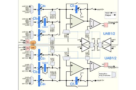
The UAB is composed of two fully symmetrical semi circuits, which can be configured as a pseudo - difference or two single - end functions. Each semi circuit is equipped with a control logic for autonomous operation. Figure 2 shows a simplified UAB diagram. UAB has a highly flexible transformation and continuous routing architecture, which can implement complex simulation functions such as analog filters.
Figure 2: simplified UAB
Charge transfer principle
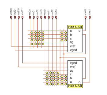
The charge transfer refers to the controlled movement of the charge between the voltage nodes. Figure 3 shows the charge transfer in the resistor and the switched capacitor.
Figure 3: simplified UAB
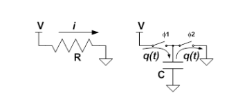
Figure 3 clock skew sequence diagram
2.Setting up time and holding time
In the resistor, the current (I) is formed by the potential difference at both ends of the resistance (R). The current flows from a voltage potential (V) to the ground potential through a resistance R. Follow the following equation:
i = V / R
In the switched capacitor, the current (I) is formed by a high potential node charging the capacitor (C) and discharging to a low potential node. When the 1 switch is closed and the 2 s switch is opened, the capacitance C is full. The charge stored is: q=CV
When the 1 switch is opened and the 2 switch is closed, all the charge stored is moved to the grounding node, and a certain amount of charge is moved within each switch period. If the control frequency of the switch is FS, the amount of charge is also moved at that frequency. The repeated movement of the charge generates a current, complying with the following equation:
i = q/t = fsq = fsCV
Unlike resistors, the current in the switched capacitor does not move continuously. By comparing the above two current equations, we will find that if they have the same voltage drop current ratio, it is equivalent to the resistor. Therefore, we can use the shunt switched capacitor to series the resistor.
V/i = R = 1/fsC
The equivalent resistance is inversely proportional to the switching frequency and the capacitance. The relative value of the resistor can be easily changed by changing the switching frequency. A higher C value means a larger current and a smaller equivalent resistance. Similarly, a higher switching frequency (FS) means a larger current and a smaller equivalent resistance. In order to produce the above results, the above results are produced by the requirements of the 1 and the 2 switches, which include:
1) Do not shut down two switches at the same time;
2) Before closing a switch, open another switch.
3) The maximum switching frequency is selected to allow the C to fully charge discharge within the cycle.
This switching capacitor forms an UAB with an operational amplifier and comparator. In this way, developers can integrate a variety of analog functions. This article explains one such simulation feature, -VDAC.
VDAC Implementation VDAC Implementation:
VDAC is a digital to analog converter, which converts digital input into an equivalent analog voltage. VDAC is the core of many control systems, which determines the performance and accuracy of the system. The accuracy of the output voltage of the VDAC ultimately depends on the reference voltage. VDAC has many applications, such as a programmable voltage generator, which provides a sensor bias and compensation voltage, a comparator reference voltage or a dynamic output waveform.
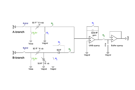
The UAB switching capacitor topology of the VDAC circuit is shown in Figure 3. Due to the discrete time property of the switched capacitor module, the switched capacitor will sample and buffer the data to obtain continuous output. This module supports working in MCU's work and sleep mode.
This topology brings flexibility to the VDAC function. The dynamic Vout range is determined by the Vref value at one end and the Vagnd value at the other end. This allows users to provide Vref and Vagnd through external circuits to set up the dynamic Vout range. In addition, the gain setting can select the output range as Vagnd+ Vref, Vagnd+ 2Vref, or Vagnd+ 4Vref, so that the full range between Vssa and Vdda is feasible. This VDAC has a 13 - bit input range from - 4096 to +4095. These values can be written directly to the corresponding register to take effect.
Figure 3: VDAC based on switched capacitor topology
The VDAC in the analog coprocessor also supports the multiplication mode. In this mode, the VDAC output voltage is multiplied by the analog input signal to form a product output. Multiplicative DAC (MDAC) is an ideal module for fixed reference applications. In such applications, users want to generate waveforms from fixed DC voltages. In addition, these MDAC are also suitable for all kinds of reference applications that users want to digitize the conversion of AC or arbitrary reference voltage.
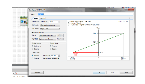
VDAC IDE To configure:
Despite the high flexibility and programmability of MCU, developers are concerned that many configuration registers and adjustment modules are needed to adapt to their application design. The PSoC Creator tool supports an analog coprocessor that allows users to configure these functions conveniently. PSoC Creator is a free Windows based integrated development environment (IDE) capable of implementing parallel hardware and firmware design systems. The design environment of the tool is similar to the Lego block, and users can place them on the circuit diagram by double clicking components and configure their functions. Figure 4 shows the VDAC component configuration tools in PSoC Creator, which can shorten the design cycle.
Figure four: the VDAC component configuration tool in PSoC Creator
The last one: How to use FPGA for time sequence analysis and design
The next one: Unmanned military systems need high precision systems