

Industry Now
HOME PAGE >
NEWS CENTER >
How to use FPGA for time sequence analysis and design
Industry Now
Release time: 2017-06-16 Author: ZLG remote electronics
FPGA(Field-Programmable Gate Array)Field programmable gate array (FPGA) is a semi custom circuit in the field of ASIC, which solves the shortcomings of custom circuit and overcomes the shortcomings of the limited number of original programmable devices. This article will give a detailed description of how time sequence is used to analyze and design with FPGA.
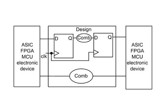
Figure 1 Basic Electronic Systems
1. Clock jitter and clock skew
The uncertain time of the change of the edge of the 1. clock jitter signal is called the clock jitter, as shown in Figure 2. In general, the time series analysis does not consider the clock jitter. If the clock jitter is considered, the time should be Tsu+T1 and the retention time should be Th+T2.
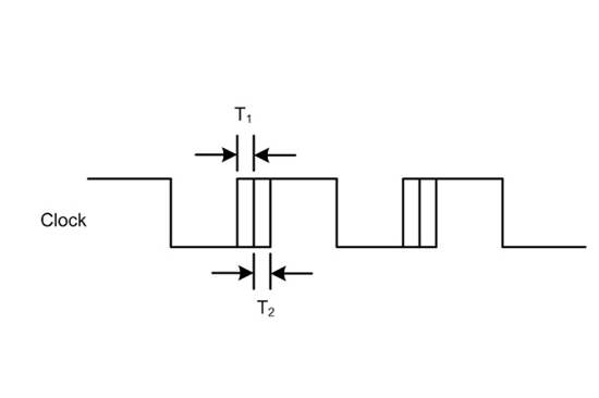
Figure 2 clock jitter sequence diagram
2. clock skew sequence skew analysis diagram
3. The starting point of the analysis of the clock is the source register (Reg1), and the destination is the target register (Reg2). The transmission of the clock in the structure of the picture will also be delayed. The time delay of transmitting the clock signal from the clock source to the source register is Tc2s, and the delay to the target register is Tc2d. The time delay of the clock network is the difference between Tc2s and Tc2d, that is, Tskew=Tc2d-Tc2s.
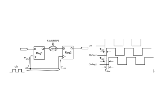
Figure 3 clock skew sequence diagram
4. Setting up time and holding time
The establishment of the time (Setup Time) Tsu said, referring to the previous at the rising edge of the clock signal trigger arrival data and enable signal constant time, if the time is not enough, the data will not be driven in the rising edge trigger clock enable signal, no effect, that is to say in this cycle of invalid data operation; holding time (Hold Time) Th said, referring to the future in the rising edge of the clock signal trigger arrival data and enable signal constant time, if the holding time is not enough, the same data cannot be scored the trigger, the operation of the data is also invalid, enable signal invalid. If data can be transmitted steadily, the relationship between time and time must be satisfied. Figure 4 identifies the relationship between them.
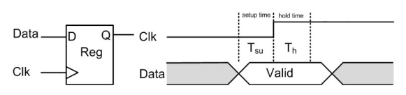
Figure 4 the concept of setting up time / time
3. The sending edge and the capture edge
(1) the sending edge (Launch Edge): the clock edge of the pre - stage register sends the data, which is the starting point of the time sequence analysis.
(2) capture the edge (Latch Edge): the back register capture the data corresponding to the clock edge, is the end of the time sequence analysis. Relative to launch Edge is usually a clock cycle, but it is not absolute, such as multiple cycles. "Signal jump to the window": for the latch register, it starts from the Hold Time corresponding to the previous clock and ends with the Setup Time of the current clock. "Signal level sampling window": for the latch register, start from the Setup Time corresponding to the current clock, to the end of the Hold Time corresponding to the current clock. The launch register must ensure that the driving signal jump to the latch register at the time of "signal jump to the arrival window", so as to ensure that the "signal level sampling window" of the latch register is not damaged. "Signal jump to the window": for the latch register, it starts from the Hold Time corresponding to the previous clock and ends with the Setup Time of the current clock. "Signal level sampling window": for the latch register, start from the Setup Time corresponding to the current clock, to the end of the Hold Time corresponding to the current clock. The launch register must ensure that the driving signal jump to the latch register at the time of "signal jump to the arrival window", so as to ensure that the "signal level sampling window" of the latch register is not damaged.
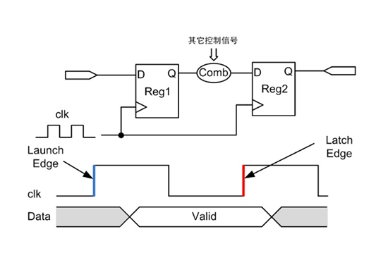
5.Launch Edge和Latch Edge
4、Four, time series analysis of data and clock
As shown in Figure 6, the basic circuit diagram for setting up time / hold time is analyzed. Tclk1 Reg1 Tclk2 Reg2 clock delay, clock delay, Tco Reg1 Tdata Reg1 the inherent delay to Reg2 combinational logic delay, Tsu Reg2 Th Reg2 setup time, hold time, set the clock cycle for T CLK, this analysis of the data of the setup time and hold time.
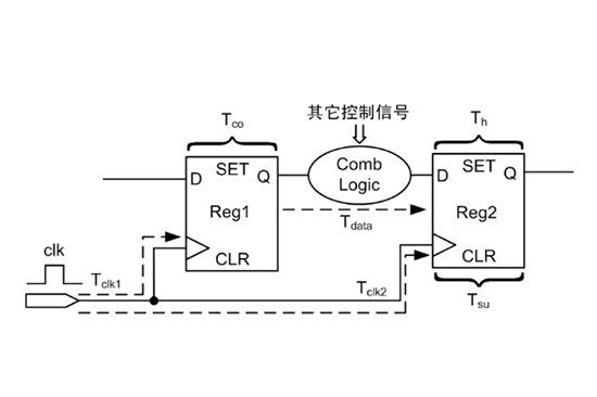
6. basic circuit diagram
1. Analysis of the establishment of time
As shown in Figure 7, the analysis of time setting is based on the first launch Edge, and the results are viewed at Latch Edge. Set up a time margin (T is a clock cycle):
Setup Stack = (T+Tclk2) – Tsu – (Tclk1+Tco+Tdata)
If T = Tclk2-Tclk1, then:
Setup Stack = (T+△T) – Tsu – (Tco+Tdata)
The delta T0 influence establishment time, the time of establishing more demanding. So for T to avoid as far as possible, using a single clock synchronization, clock signal and try to use the global, so T is almost 0, and effect of delta T almost does not exist, can be ignored.
If the establishment time margin Setup Stack is less than 0, then the establishment time will not be satisfied, and the unstable state will be produced and transmitted through the register.
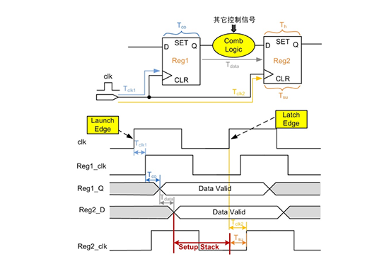
Figure 7 set up a time sequence analysis diagram
2. Analysis of the retention time
As shown in Figure 8, the analysis of the retention time is based on second launch Edge, and the results are viewed at Latch Edge. Keep the time margin:
Hold Stack = (Tclk1+Tco+Tdata) – Tclk2 – Th
hypothesis△T = Tclk2-Tclk1,Then:
Hold Stack = (Tco+Tdata) – △T – Th
The delta T>0 effect of hold time, keep time more demanding.. So for T to avoid as far as possible, using a single clock synchronization, clock signal and try to use the global, so T is almost 0, and effect of delta T almost does not exist, can be ignored. If the margin of the retention time Hold Stack is less than 0, the holding time will not be satisfied, and the unstable state will be produced and transmitted through the register.
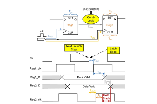
Figure 8 holding time sequence analysis diagram
Five, DT6000S project example
On the DT6000S project, 4 Optical Ethernet interfaces are connected to FPGA, and SV and GOOSE are implemented by FPGA to implement the MAC layer and decode IEC61850. Ethernet PHY passes through the MII interface and FPGA, so there are 4 MII interfaces between FPGA and the external interface. The initial stage of the project is to realize the 1 way optical Ethernet interface. After verification function is correct, there will always be 1 way optical Ethernet communication is not normal when the 4 way Ethernet is turned into later. After analysis, the time sequence of the FPGA pass MII interface and the PHY is not satisfied. As shown in Figure 9 as a sequence diagram of the MII interface, time series is not satisfied to be divided into TX_CLK and RX_CLK.
One is that the TX_CLK and FPGA output from PHY are large based on the TXD[3:0]&TX_EN generated by TX_CLK, and the main delay is internal logic delay. PCB delay is small and consistent, resulting in the establishment time of PHY TX_CLK is not satisfied, resulting in sending data errors.
The second is the difference between the delay of PHY's output RX_CLK and RXD[3:0]&RX_DV&RX_ER to FPGA's internal synchronous trigger is too large, which leads to the establishment time of RX_CLK of internal synchronous trigger of FPGA is not satisfied, resulting in receiving data error. Therefore, FPGA needs to add constraints to meet the requirements of the timing, and the constraints are TXD[3:0] and TX_EN with less output delay. The difference between the RX_CLK and RXD[3:0]&RX_DV&RX_ER path delays is small. After the constraints are added, the optical Ethernet data communication of the 4 MII interface is normal.
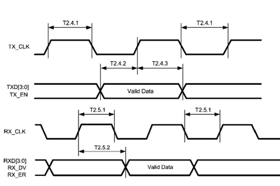
Figure 9 MII sequence diagram
In this paper, the basis of time series analysis is expounded, the time series analysis is carried out at the same time, and the time and the time of maintenance are understood by the time series analysis. It is hoped that after reading this article, we can have a further understanding of the FPGA sequence analysis.
The last one: Semiconductor manufacturers compete for video surveillance market
The next one: Using intelligent simulation module for design